


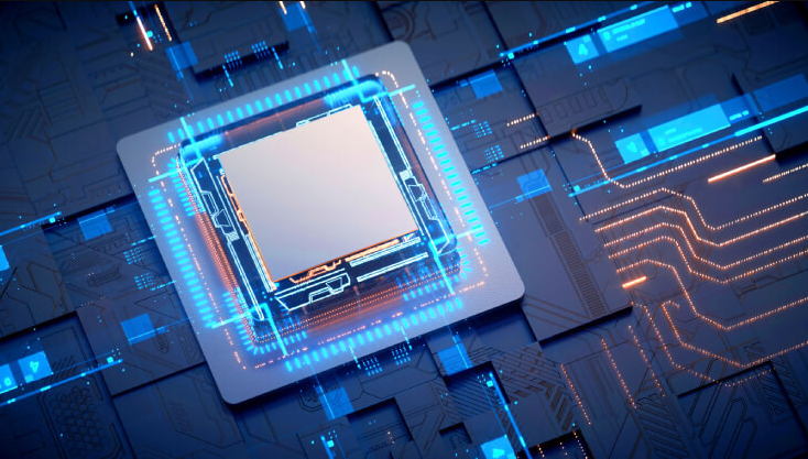
New Chipset Innovations Reshaping 2025: From 2 nm Nodes to Modular AI Architectures
💡 Key Innovations in Chipset Development (2025)
🏭 1. MediaTek’s 2 nm Chipset on the Horizon
At Computex 2025, MediaTek confirmed that it will tape out its first 2 nanometer chip this September, built via TSMC. This next‑gen chipset—designed for high-volume applications—promises around 15% better performance and 25% improved power efficiency compared to its 3 nm predecessor. It’s also centered around embedded AI capabilities for tasks like real-time language translation, smart voice interfaces, autonomous driving, and next-generation 6G networks Laptop Mag+15Business Today+15spectalks.com+15.
🎛️ 2. Advance in Gate-All-Around (GAA) and Backside Power Delivery
By 2025, chipmakers including TSMC, Samsung, Intel, and Japan’s Rapidus are scaling GAAFET transistor architectures, paired with backside power delivery, to push energy efficiency and transistor density even further. This combination is foundational to modern process nodes (<2 nm) and is expected to go into mass production soon ING Think+1Wikipedia+1.
🧩 3. Modular, Chiplet-Based Designs
The industry is accelerating modularity: UCIe 2.0, released in August 2024, standardizes chiplet interconnection across ecosystems like AMD, Intel, TSMC, Qualcomm, and others. Support for 3D packaging and real-time system health monitoring now enables scalable, heterogeneous architectures for AI, HPC, and edge devices Wikipedia.
Additionally, Huawei’s patent for a quad‑chiplet architecture for its rumored Ascend 910D accelerator rivals Nvidia’s design—highlighting global momentum behind modular packaging for high-performance AI systems Tom’s Hardware.
🤖 4. AI-Accelerated Chip Design & EDA Integration
Synopsys’s $35 billion merger with Ansys merges electronic design automation with multiphysics simulation, enabling AI-driven chip design workflows. This unified platform lets developers simulate entire system behavior before manufacturing—a significant leap in speed and accuracy for color, thermal, and structural chip validation Tom’s Hardware.
Top research firms like imec are advocating programmable AI-centric chip architectures featuring modular supercells and on‑chip networks supporting 3D stacking—ensuring future-proof hardware for evolving AI models Reuters.
🏭 5. Japan’s Return to Leading-Edge Fabrication
Japanese foundry Rapidus began active test production of 2 nm transistors at its IIM‑1 facility. Its single-wafer processing approach delivers fine process control and data-rich yields. Mass production is pegged for 2027, positioning Rapidus as a national champion in advanced node development infosys.com+4Tom’s Hardware+4Wikipedia+4.
🚀 6. Connectivity & Networking Chip Advances
Broadcom’s Tomahawk Ultra, launched July 15, 2025, acts as a high-speed networking engine to interlink hundreds of AI accelerators within data centers. It leverages enhanced Ethernet protocols and scales up to connect four times more chips than Nvidia’s NVLink Switch, enabling massive scale compute clusters for generative AI workloads Reuters.
🔍 Why This Matters
| Innovation Area | Impact Summary |
|---|---|
| 2 nm & GAA Nodes | Enable major gains in power efficiency and computing density |
| Chiplet & Packaging | Power modular, scalable systems with flexible integration |
| AI-Driven Design Tools | Accelerate chip development for complex systems |
| Networking Processors | Support massive compute scaling for AI applications |
These innovations collectively mark a major leap in how chipsets will be designed, produced, and deployed across computing, AI, telecom, automotive, and IoT applications.